Verilog RAM RTL code. Reg 40 ROM 630.

Verilog Code For Ram Youtube
Languages HDLs provide a more compact textual description of a design.
. Figure 1 shows a. Create a Verilog HDL design that instantiates the function. Type your Verilog code Memory_SPv in the new window.
Module ram_singleq a d we clk. You probably couldnt write a decent novel if youd never read a novel. This book attempts to capture the spirit of the Bronze Age of video games when video games were designed as circuits not as software.
Set the desired design as top-level. This page covers RAM verilog code and ROM verilog codeIt also provides link which compares RAM vs ROM. For loading data into ROM from a file refer to this link.
To instantiate a RAM or ROM function in Verilog HDL follow these steps. Rom_using_file 3 File Name. Always addr case addr 8d0.
This revised edition of DKs groundbreaking 2003 atlas has been refreshed with beautiful bright new maps a topic. Synchronous Random Access Memory RAM implementation in Verilog. Each section shows the list of Verilog-files require to implement the design in that section.
Teach Yourself Verilog With This Tiny CPU Design. Assign dout dout_r. Implement synchronous RAM Random Access Memory and also provide a test-bench to validate it.
The example below shows ram_singlev a Verilog Design File that implements a 128 x 8-bit synchronous single-port RAM with common read and write addresses. End But you should use Macro from FAB if youre going to synthesize real ASIC. ROM using readmemh 5 Coder.
Since 64-bit x 8-bit memory is considered here 64-bit address is considered and the main goal is to input 8-bit data that should be written in this address location. So prefer using mixed block array. 1 ----- 2 Design Name.
Designing Video Game Hardware In Verilog. Designing a ROM block ie a sequential circuit that can perform different mathematical function. Coefficient Multiplier always posedge clk c RAM - flow through if c_ram_en if c_ram_wr begin c_RAMi.
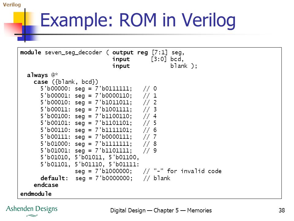
Verilog Digital Design Chapter 5 Memories 16 Example. Always posedge clk y register if y_ce begin if mult_sel begin operand1 c_out. Use the genmem utility to generate a memory model by typing the following command at the UNIX prompt.
Implement combinational and sequential. End Or reg 40 ROM 630. 6111 Spring 2006 Introductory Digital Systems Laboratory 13 Block ROM using Verilog Code Asynchronous Block ROM module rom addr data.
17 18 reg 70 mem 0255. Childrens World Atlas With CDROM 9780756675844 0756675847. Verification ambiance may be able application System Verilog after application any accurate methodology but that will be different for every distortion of the design.
Designing rom in verilog It is easier than straightforward to develop exceptional nail artwork for short nails. Verilog HDL Fundamentals for Digital Design and Verification. A Guide to Digital Design and Synthesis With CDROM Hardcover ed 0130449113 9780130449115.
Navabis Verilog textbook introduces the Verilog hardware description language and its use in digital circuit and system design and modeling in a comprehensive manner. Design module single_port_sync_ram parameter ADDR_WIDTH 4 parameter DATA_WIDTH 32 parameter DEPTH 16 input clk. As follows refer to Verilog slicing link for further information.
In the structural level more abstract assign statements and always. Designing Rom In Verilog. A much-needed step-by-step tutorial to designing with Verilog--one of the most popular hardware description languages Each chapter features in-depth examples of Verilog coding culminating at the end of the book in a fully designed central processing unit CPU CD-ROM featuring coded Verilog design examples A first-rate resource for digital designers computer designer engin.
ROM in verilog If you use ROM for emulation you can use this construct for example. Y is necessarily a constant. His approach to study of the language spans all design methodologies including structural behavorial and.
234 6 40MB Read more. Lastly all designs are tested using Modelsim and on Altera-DE2 FPGA board. I dont know if youre asking for detailed Verilog code to implement a simple audio player but since your question didnt include an offer to pay for engineering services or an employment offer in your company to do this work Ill assume that you are asking how to approach the.
Home Interview Basics Design RTL VLSI Python LTE. End else c_out. The lowest level is the gate level in which statements are used to define individual gates.
Answer 1 of 2. Differentiate between Verilog structural dataflow behavioral design styles and how when to use them in Digital Design and Verification. Learning to do something often involves studying what other people did.
14 output 70 data. Note that these inputs are arbitrary and you can enter any 8-bit data. Introduction to Verilog Chip Design Flow Chip Abstraction Layers Data Types Verilog Syntax Verilog Data types Verilog ScalarVector Verilog Arrays Building Blocks.
Well delve into these circuits as they morph from Pong into programmable personal computers and game consoles. Deepak Kumar Tala 6 ----- 7 module rom_using_file 8 address Address input 9 data Data output 10 read_en Read Enable 11 ce Chip Enable 12. All youll want to do will be to introduce some glitter in.
Endcase endmodule ROM delay. Rom_using_filev 4 Function. Master the basics of Verilog language for designing synthesizable digital circuits for ASIC FPGA.
- GitHub - anupkumar-siucROM-Memory-Design-Using-Verilog. Always posedge clk begin if we mema. Following is the figure and verilog code of RAM Random Access Memory.
Verilog is a powerful language and offers several different levels of descriptions. There is no difference or perhaps a little difference between using packed and unpacked arrays. Y the start position is x and count down from x by Y.
All the design files are provided inside the VerilogCodes folder inside the main project directory. RAM Verilog Code ROM Verilog Code. Which can be used to implement the design using some other software as well.
Reg 70 mem 1270. Alwaysnegedge reset ifreset begin ROM0. 13 input 70 address.
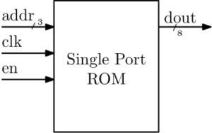
Memory Design Digital System Design

Verilog Code For Rom Youtube
2

Ram Verilog Code Rom Verilog Code Ram Vs Rom

Design Of Rom In Verilog Youtube

Verilog Tutorial 05 Simple Rom Youtube
Digital Design An Embedded Systems Approach Using Verilog Ppt Video Online Download

Ram Verilog Code Rom Verilog Code Ram Vs Rom
0 comments
Post a Comment